This is a simple powered speaker that was originally intended to be used as a simple piece of test equipment. It is based around a small full-range loudspeaker that I'd inherited, which originally came from Radio Spares.
The basic idea was to mount it in a diecast aluminium box, treated to make it as acoustically ideal as possible. Then add a simple amplifier using active equalisation to extend the low frequency response and make the sound acceptable. The unit was intended to be used when servicing audio equipment, but since building this project, I finally managed to fit a pair of phono sockets into the workshop connection panel for doing exactly this...
Enclosure Design:
The drive unit (RS part number 433-309) isn't stocked any more. It's described as a 3 inch 20W 4 ohm full range speaker, but that's all I knew - RS don't even suggest a manufacturer. It's quite well-made, having a large magnet and a treated paper cone with a foam surround and a plastic dust cap to extend the h.f. output. Before proceeding any further, I had to measure the basic TS parameters:
| Fs | 93 | Hz |
| Qms | 2.89 | |
| Qes | 0.69 | |
| Qts | 0.55 | |
| Vas | 1.57 | Litres |
Next I measured the volume of my spare diecast boxes. Putting these values and the above TS parameters into a calculator showed that the best box to use was one with a volume of 1.59 litres, which would provide a -3dB point of 120Hz, with a system Q around 0.78 - and while writing up this project I took the time to confirm these numbers with WinISD, which was useful confirmation.
The next problem to consider was treating the box. Try the "knuckle test" with the next diecast box you find and you'll find it rings like a bell! Clearly no good for a speaker enclosure. To stop this, I applied a layer of self-adhesive bitumen based damping material, available at car accessory shops. This transformed the box into an acoustically dead enclosure - I must admit that I was rather surprised at just how effective this was...
Next I mounted the speaker into the box. It took a while to get a good clean circular cut-out, but it worked out ok in the end. The box was pre-finished with the grey nylon coating that you can see in the pictures, so I couldn't scratch or damage this. I also mounted the phono socket so that I could connect the speaker to an amplifier.
At this point, the system resonance was 140Hz, not too far from the prediction (which didn't include the volume taken by the driver). I added some stuffing, which lowered the resonance to 132Hz - this works because it causes the driver to "see" a larger volume of air. Next I sealed the box, as I thought I could hear some tiny air leaks, which brought the system resonance down to 128Hz.
Listening to the driver directly from the workshop hi-fi, I was surprised at how good this cheap drive unit sounded. Don't get me wrong, I'm not claiming this was hi-fi or anything, but certainly better than you might expect, and there was no hint of extraneous noises coming from the enclosure. So the next stage was to experiment with the electronics - for this I just used solderless prototype board and played around until I was happy with the sound.
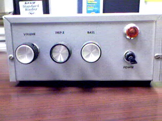
And here's the final result. From left to right, there's the input connector (gold-plated, so it must sound good ;-), the volume and tone controls, the green power LED and the red clipping LED.
And here are some internal views, showing the damping material and stuffing. Note the gaskets around the driver opening and the edge of the box - as mentioned, these proved to be very necessary. The bass quality can be heard to improve as the screws are tightened! There's similar gaskets surrounding the IEC socket and mains fuse.
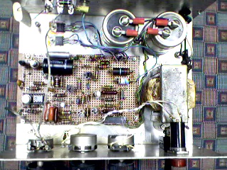
This is a closer view of the electronics. The power IC is bolted to a 6mm piece of aluminium, which is held to the front of the box by the potentiometers. The expensive blue pots were the only things I could find with long enough bushes to reach through the aluminium and the front panel - luckily they were "recycled"! The two LED's are connected to the brown wires, and held in place by a small piece of damping material which also stops air leaks.
Circuit Details:
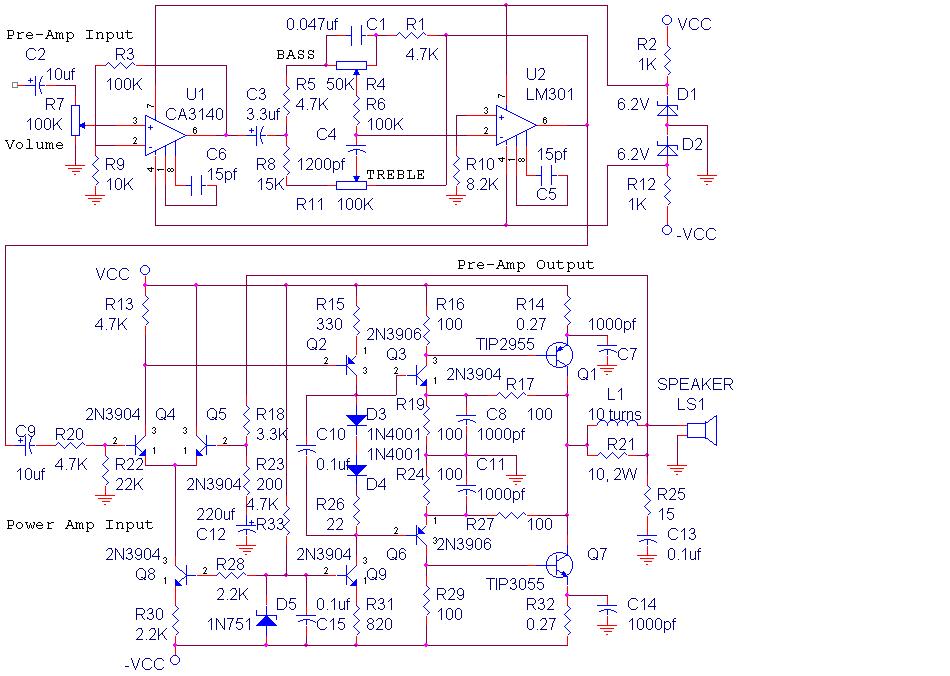
The electronics is based around a dual op-amp (LM833) and TDA2030 power amp IC. Click the thumbnail to view the complete schematic..
As you can see, it's mostly straightforward stuff, although there are one or two unusual bits, such as the tone control and frequency shaping section, and the clipping detector.
Input buffer:
This is the input section, starting with an ultrasonic filter that turns over at around 150kHz with typical source impedances. This is just a simple (and essential) measure to stop the input op-amp picking up cellphone noise, etc. From the volume control, the non-inverting op-amp stage has a voltage gain of 20dB. The low frequency -3dB point of this stage is around 13Hz - this might seem unreasonably low for such a small speaker, but the system LF behaviour is formally set by the next stage...
High-Pass Filter:
Directly after the input buffer is the high-pass filter. This is a second-order Bessel filter, chosen for its superior in-band phase response and step-response, compromising on flatness of frequency response, which is pretty academic with this sort of loudspeaker. Chapter 5 of The Art of Electronics by Horowitz and Hill gives a really good introduction to active filters
With the values shown, it turns over at 75Hz. The output from the speaker has fallen by about 10dB at this frequency, so there's little benefit to feeding lower frequencies into it - this will just waste energy.
Tone Control and Equalisation:
Following on from the HPF stage is the tone control and equalisation section. This might look slightly strange at first, but the basic idea is to use capacitors to shape the frequency response.
The 22K resistor forms a potential divider with the 4K7 resistor (the one connected to ground). At mid-range frequencies the 2n2 capacitor is open-circuit, and the 120n capacitor is short-circuit. Therefore the attenuation is around 15dB.
But the 4K7 and 2n2 combination bypasses the 22K resistor at high frequencies, providing treble boost. Assuming the capacitor looks more like a short-circuit, the attenuation is only 6dB, or in other words, there is a HF lift of around 9dB.
The 4K7 and 120n combination provide bass boost in a similar fashion. At bass frequencies, the 120n capacitor looks more like an open-circuit, meaning that the 4K7 resistor does not play a part in the potential divider. As the impedance of the next stage is 22K, the attenuation here is also 6dB, so there's a 9dB bass lift...
The tone control is able to remove this bass boost by short-circuiting the 120n capacitor (with the control full clockwise). When the control is fully anticlockwise (bottom of diagram), the 22n capacitor is connected in series with the 120n capacitor to the bottom half of the potential divider, effectively cutting the HF response. With the control in the centre position, it doesn't really play a significant part in shaping the response of the bass and treble boost circuits.
Just to prove all this works, here's a simulation of the complete circuit showing the gain from the input right up the output of this stage. The power amplifier is excluded as this can be assumed to have a flat frequency response. Click the image to see a larger version...
The white trace is the response with the tone control in the centre position, the green trace shows the treble-cut achieved with the tone control at minimum, and the blue plot shows the bass-cut that occurs when the tone control is set to maximum. The simulations confirms the numbers discussed above, which were "worked out on the back of an envelope".
This sort of frequency response shaping used to be very popular with transistor radios and TV sets in the "good old days". Ever wondered why old Roberts and Grundig radios sound so nice? Unfortunately, many manufacturers don't seem to bother these days...
Power Amplifier:
The power amplifier stage is pretty much straight from the datasheet. The gain is 11 (21dB), but the 22uF capacitor reduces the gain to unity at DC to prevent DC offsets appearing across the voicecoil. This measure is less necessary with newer chip-amps like LM1875's, etc, so it's common to see this component omitted. The 1n4001 diodes are 'catch' diodes to prevent the inductive load of the loudspeaker causing voltage spikes that might be greater than the supply rails - again these are much less necessary with modern chip-amps that employ measures like "SPiKe" protection - check the datasheets carefully. The amplifier is decoupled with 100n capacitors mounted next to the IC, and as the main power supply capacitors are only a few centimetres away from the IC, this is perfectly acceptable. Finally, there is a Zobel network to ensure the amplifier remains stable with the inductive load of the loudspeaker. This also improves the amplifiers susceptibility to RF ingress.
Clipping Detector:
Finally, this is the clipping detector. I had some spare space on the circuit board, and this was an idea that I'd wanted to try for some time now...
The basic problem with conventional clipping detectors is that they trigger at some preset absolute threshold - which doesn't take into account the actual values of the supply rails. As power amplifiers are most often supplied by unregulated power supplies, this is a serious shortcoming. The detector threshold would have to be set up to trigger during worst-case instances of low mains supply and maximum supply voltage sag. But under more favourable conditions, the clipping indication could be triggering several dBs below maximum output.
So this design responds to the
difference between the output signal and the supply voltages. Under normal operating conditions, both transistors are conducting, and the LED inside the opto-coupler is on. This means the transistor in the opto-coupler is on, so the BC548 and red LED are both off.
Should the output get within around 2V of either supply rail, the appropriate transistor will switch off. This means the opto-coupler LED will extinguish, hence the 27K resistor can supply base current to the BC548, turning the clipping light on.
This circuit could be improved in a number of ways. For a start, there is no form of "pulse stretching", so very brief transients or HF clipping might not be seen. As there is so much bass boost in the preamp and no tweeters to burn out, I didn't worry about this here. Also, it is relatively tricky to adjust this circuit to respond to different power amplifiers - not all of them can actually get to within 2V of the supply rails under all load conditions. In addition to the resistor values, the number of 1n4148 diodes determine this threshold - adding another diode to each subtracts around 0.6V from the threshold. This is fine at the prototype stage, but a pain to adjust once you've etched the PCB!
Since building this, I've found a similar circuit on Rod Elliots site. Compared to my circuit, I think that the comparator makes it slightly more complicated - I much prefer my opto-coupler arrangement. But I think that the arrangement of the detector transistors is probably better because they can switch off faster, hence it will respond to HF clipping more effectively. Not an issue for this application, but I will be investigating this when I start the power amps for my ATC's
Want to build one?
Following a recent request from an interested constructor, I've scanned the diagram of the Veroboard layout that I designed while building the unit. The original pencil drawing had plenty of corrections as it evolved, so it isn't the clearest diagram in the world. There are no component markings - at the time, the circuit was "in my head"; labels would have just cluttered the diagram.
Also note there are small differences between this drawing and the actual unit - this is because of possibilities which become apparent at the construction stage, obviously there's no point modifying the drawing at that stage because this was a one-off. The track cuts are signified in two ways - most obviously the "X", but also (indirectly) the lines drawn I've drawn to show continuous tracks. Take care, because I've just spotted a missing X!
There are circuit differences too. The layout shows two diodes per transistor for the clipping detector, but on testing, I decided to reduce this. Also, I planned to have Zener diodes to regulate the supply to the op-amp, but these weren't needed in practice. Stick with the LM833 - others might produce pops and bangs when switched on/off (certainly TL082's did, but that's not unusual IME). And be realistic - NE5532's or OPA2134's would be complete overkill! Obviously, the clipping detector is optional.
I'd strongly recommend you follow my approach: build the speaker into a box, and experiment with solderless prototype board until you're happy with the sound. For example, a larger drive unit might benefit from a lower frequency HPF (increase the 82n capacitors). The deliberate dip in the midrange designed to suit my small driver might cause better drivers to lack "presence", in which case, alter the component values around the tone control. Having said that, this EQ should make most non-hi-fi speakers sound bearable, or even "nice"!
Regarding mechanical issues, the aluminium bar was used principally to avoid visible fixings on the front panel - the TDA2030 bolts to the bar, and the bar is held in contact with the case by the two potentiometer bushes. Feel free to omit the bar if you don't mind the screwhead on the front panel, although note that this makes servicing more difficult. Don't forget to insulate the tab of the IC from the case, as it's connected to the negative supply rail. If the front panel is wood, you must arrange for some form of heat sink for the IC - although it can be tested briefly with no heat sink, it must be cooled effectively in use. Should it overheat and fail internally, it will probably destroy the loudspeaker!
If you're tempted to make changes to the layout, don't! Especially don't alter the earthing or power supply arrangements! Doing so will lead to an increase in distortion or maybe even cause the amplifier to "hum". Finally, I'd recommend that you build this very carefully, working your way logically through the circuit as you go. Don't just blindly follow the layout - like me, you'll need to have the circuit in your head (being forced to work out the component values will help here). While this circuit is not complicated, and it doesn't look particularly cramped, there was a lot of work to fit the circuit onto the board. Moving things just one hole might stop other things fitting!
Despite the above, it's not too difficult really. If anyone succeeds in making this work, please send me details of your version, and a picture or two. Good luck!
Click the image for a larger version.


